

PCI-1802L/S
330KS/s, Low Gain 12-bit, 32 Channel Analog Input, 2 Channel D/A, Digital I/O Board (8K word FIFO). Includes DB-1825 Daughter Board and Cable

Features
 The PCI-1800/1802 (L/H) is a family of high performance data acquisition board with 5V PCI bus. The PCI-1800/1802LU/HU card has a universal PCI interface supporting both 3.3 V and 5 V PCI bus. All the members in the PCI-1800 family have the same architecture; they feature a continuous A/D acquisition function of up to 330 kHz for low gain (44 kHz for high gain) under DOS and offer two 12-bit D/A output channels, 16 digital input channels and 16 digital output channels. The PCI-1800 series provides 16 single-ended or 8 differential inputs while the PCI-1802 series provides 32 single-ended or 16 differential inputs. In addition, an amazing A/D channel scan function called “MagicScan” is provided for users to easily implement multi-channel analog data acquisition applications. The specific MagicScan controller takes out most works of getting A/D value such as selecting channel, setting gain, settling time, triggering ADC and getting data. Even in channel scan mode, it can have different gain code for each channel, and the sampling rate can still reach 330 kS/s totally. The PCI-1800 series is suitable for high end applications.
The PCI-1802 series cards are equipped with 8 K samples hardware FIFO to reduce data overflow issues under multi-tasking environment like Windows and Linux.
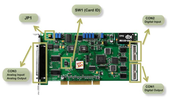
The PCI-1800/1802LU/HU has a Card ID switch with which users can recognize the board by the ID via software when using two or more PCI-1800/1802LU/HU cards in one computer. The pull-high/low jumpers of the card allow user to predefine the DI status instead of floating when the DI channels are unconnected or broken.
The PCI-1800/1802 series cards support Linux, DOS, Windows 98/NT/2000, and 32/64-bit Windows XP/2003/2008/Vista/7. The I/O card SDK provides DLL, Active X control and sample programs with source codes of various languages such as Turbo C, Borland C, Microsoft C, Visual C++, Borland Delphi, Borland C++ Builder, Visual Basic, C#.NET, Visual Basic.NET and LabVIEW . Users can refer to the demos for their development tool to implement application quickly and easily.
ICP DAS discontinues the /NDA model (without D/A function) since the standard model provides full functions that covers the requirement for /NDA version. Please contact us for OEM/ODM project if you are interested in customized version (or /NDA model).
- PCI bus, 5 V, 32-bit, 33 MHz for PCI-1800/1802L/H
- 12-bit 330 kHz A/D converter
- AI channels:
16 single-ended/8 differential inputs, 1 K word FIFO buffer for PCI-1800 series
32 single-ended/16 differential inputs, 8 K word FIFO buffer for PCI-1802 series - Total sampling rate:
up to 330 K samples/s for low gain model
up to 44 K samples/s for high gain model - Programmable gain:
Low gain: 0.5, 1, 2, 4, 8 for PCI-1800/1802L/LU
High gain: 0.5, 1, 5, 10, 50, 100, 500, 1000 for PCI-1800/1802H/HU - Three different external trigger: post-trigger, pre-trigger, middle trigger
- Internal/external A/D trigger
- 16 digital input/16 digital output channels
- Two 12-bit DA channels, 2 MHz throughput per channel (max.)
- High speed data transfer rate up to 2.7 Mword/sec.
- DB-889D accessory for expanding channels of PCI-1800 series
- DB-889D and DB-1825 accessories for expanding channels of PCI-1802 series
- Half size board
[PCI-1800/1802LU/HU only] - Universal PCI interface supports both 5 V and 3.3 V PCI bus.
- Pull-high/ pull-low resistors for DI channels.
Applications
- High speed data acquisition system
- Process monitor and control.
- Vibration analysis.
Software
- DOS Lib and TC/BC/MSC sample program (source codes included)
- DLL and OCX SDK for Windows 98/NT/2000.
- DLL and OCX SDK for 32-bit and 64-bit Windows XP/2003/Vista/7.
- VB/VC/Delphi/BCB/VB.NET/C#.NET/VC.NET/MATLAB sample programs with source codes.
- LabVIEW toolkit for Windows.
- Driver for Linux.
Specifications
| Model Name | PCI-1802H PCI-1802L |
PCI-1802HU PCI-1802LU |
PCI-1800H PCI-1800L |
PCI-1800HU PCI-1800LU |
|||||||||||||||||||||||||||||||||||||||||||||
| Analog Input | |||||||||||||||||||||||||||||||||||||||||||||||||
| Channels | 32 single-ended/16 differential | 16 single-ended/8 differential | |||||||||||||||||||||||||||||||||||||||||||||||
| AD Conversion | 12-bit, 3 μs conversion time | ||||||||||||||||||||||||||||||||||||||||||||||||
| Sampling Rate | 330 kS/s. max. | ||||||||||||||||||||||||||||||||||||||||||||||||
| FIFO Size | 8192 samples | 1024 samples | |||||||||||||||||||||||||||||||||||||||||||||||
| Over voltage Protection | Continuous +/-35 Vp-p | ||||||||||||||||||||||||||||||||||||||||||||||||
| Input Impedance | 10 MΩ/6 pF | ||||||||||||||||||||||||||||||||||||||||||||||||
| Trigger Modes | Software, Internal programmable pacer, External (5 V/TTL compatible) | ||||||||||||||||||||||||||||||||||||||||||||||||
| Data Transfer | Polling | ||||||||||||||||||||||||||||||||||||||||||||||||
| Accuracy | 0.01 % of FSR ±1 LSB @ 25 °C, ± 10 V | ||||||||||||||||||||||||||||||||||||||||||||||||
| Zero Drift | +/- 2 ppm/°C of FSR | ||||||||||||||||||||||||||||||||||||||||||||||||
| Analog Output | |||||||||||||||||||||||||||||||||||||||||||||||||
| Channels | 2 | ||||||||||||||||||||||||||||||||||||||||||||||||
| Resolution | 12-bit | ||||||||||||||||||||||||||||||||||||||||||||||||
| Accuracy | 0.06% of FSR ± 1 LSB @ 25 °C, ± 10 V | ||||||||||||||||||||||||||||||||||||||||||||||||
| Output Range | Bipolar:+/5 V, +/-10 V | ||||||||||||||||||||||||||||||||||||||||||||||||
| Output Driving | +/- 5 mA | ||||||||||||||||||||||||||||||||||||||||||||||||
| Slew Rate | 8.33 V/μs | ||||||||||||||||||||||||||||||||||||||||||||||||
| Output Impedance | 0.1 Ω max. | ||||||||||||||||||||||||||||||||||||||||||||||||
| Operating Mode | Software | ||||||||||||||||||||||||||||||||||||||||||||||||
| Dgital Input | |||||||||||||||||||||||||||||||||||||||||||||||||
| Channels | 16 | ||||||||||||||||||||||||||||||||||||||||||||||||
| Compatibility | 5 V/TTL | ||||||||||||||||||||||||||||||||||||||||||||||||
| Input Voltage | Logic 0: 0.8 V max. Logic 1: 2.0 V min. |
||||||||||||||||||||||||||||||||||||||||||||||||
| Response Speed | 2.0 MHz (Typical) | ||||||||||||||||||||||||||||||||||||||||||||||||
| Digital Output | |||||||||||||||||||||||||||||||||||||||||||||||||
| Channels | 16 | ||||||||||||||||||||||||||||||||||||||||||||||||
| Compatibility | 5 V/TTL | ||||||||||||||||||||||||||||||||||||||||||||||||
| Output Voltage | Logic 0: 0.4 V max. Logic 1: 2.4 V min. |
||||||||||||||||||||||||||||||||||||||||||||||||
| Output Capability | Sink: 2.4 mA @ 0.8 V Source: 0.8 mA @ 2.0 V |
||||||||||||||||||||||||||||||||||||||||||||||||
| Response Speed | 2.0 MHz (Typical) | ||||||||||||||||||||||||||||||||||||||||||||||||
| Timer/Counter | |||||||||||||||||||||||||||||||||||||||||||||||||
| Channels | 3(Independent x 1/Internal pacer x 1/External pacer x 1) | ||||||||||||||||||||||||||||||||||||||||||||||||
| Resolution | 16-bit | ||||||||||||||||||||||||||||||||||||||||||||||||
| Compatibility | 5 V/TTL | ||||||||||||||||||||||||||||||||||||||||||||||||
| Input Frequency | 10 MHz max. | ||||||||||||||||||||||||||||||||||||||||||||||||
| Reference Clock | Internal: 8 MHz | ||||||||||||||||||||||||||||||||||||||||||||||||
| General | |||||||||||||||||||||||||||||||||||||||||||||||||
| Bus Type | 5 V PCI, 32-bit, 33 MHz | 3.3 V/5 V Universal PCI, 32-bit, 33 MHz |
5 V PCI, 32-bit, 33 MHz | 3.3 V/5 V Universal PCI, 32-bit, 33 MHz |
|||||||||||||||||||||||||||||||||||||||||||||
| Data Bus | 16-bit | ||||||||||||||||||||||||||||||||||||||||||||||||
| Card ID | No | Yes(4-bit) | No | Yes(4-bit) | |||||||||||||||||||||||||||||||||||||||||||||
| I/O Connector | Female DB37 x 1 Male 20-bit ribbon x 2 |
||||||||||||||||||||||||||||||||||||||||||||||||
| Dimensions (L x W x D) | 200 mm x 105 mm | ||||||||||||||||||||||||||||||||||||||||||||||||
| Power Consumption | 300 mA @ +5 V | ||||||||||||||||||||||||||||||||||||||||||||||||
| Operating Temperature | 0 ~ 60 °C | ||||||||||||||||||||||||||||||||||||||||||||||||
| Storage Temperature | -20 ~ 70 °C | ||||||||||||||||||||||||||||||||||||||||||||||||
| Humidity | 5 ~ 85% RH, non-condensing | ||||||||||||||||||||||||||||||||||||||||||||||||
|
|||||||||||||||||||||||||||||||||||||||||||||||||
|
|||||||||||||||||||||||||||||||||||||||||||||||||
References and Support
Customer Reviews (0)
Be the first to leave a review.


...
$1,269.00 Each
Quantity added:


